
A transistor is a key electronic component used in devices like smartphones and TVs. It has three terminals—base, emitter, and collector—and functions as both an amplifier and a switch. This article covers the basics of transistor types, their structure, and how they work in electronic circuits.
With the use of transistors, it has become possible to design electronic devices that are smaller in size, have less power dissipation, and more. Examples include modern smartphones, televisions, etc.
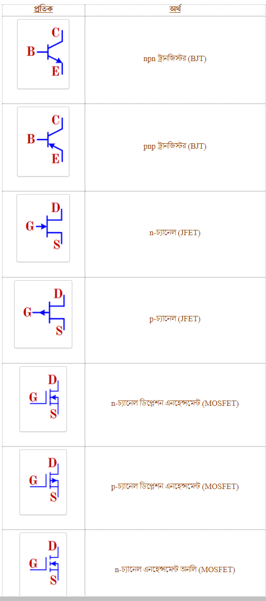
What is a Transistor and its Symbol?
The transistor is a widely used electronic device. It is a semiconductor device with three terminals, three layers, and two junctions that amplify input signals and solve various tasks. It can also function as a switch in circuits.
Symbol:

What is a Transistor Made of?
A transistor is an active semiconductor device made of semiconductors. It consists of two junctions. It can be either NPN or PNP type. It has three terminals, which we will discuss in detail shortly.
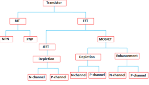
Types of Transistors
It is difficult to classify transistors precisely because modern research is constantly introducing new types. A preliminary classification of transistors is shown in the Tree Diagram below.
How Does a Transistor Work?
We already know that a transistor mainly amplifies or switches. When a small current flows through the input of a transistor, it amplifies it at the output and can also behave like a switch.
The input of a transistor typically refers to the base of a common transistor, while the output refers to the collector and emitter. However, in the case of a MOSFET, the input would be the drain and the output the source.

What Does a Transistor Do in a Circuit?
For example, in a radio, a transistor acts as an amplifier. Electromagnetic waves, which are very low in strength, are amplified by the transistor through the proper circuit, and the sound reaches our ears via a speaker.
Construction of NPN and PNP Transistors
NPN Transistor (npn)
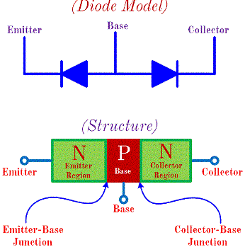
An NPN transistor is formed by placing a P-type semiconductor between two N-type semiconductors, creating a P-N junction.
The image shows that the transistor has three terminals. The same type of region (N) forms the emitter and collector, while the opposite region (P) forms the base.
Thus, in the case of an NPN transistor, the base is a P-type region, and the emitter and collector are N-type regions. The junction between the collector and base is called the collector-base junction, while the junction between the emitter and base is called the emitter-base junction.
PNP Transistor (pnp)
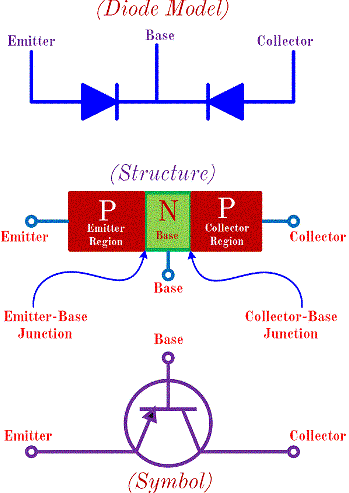
This is essentially the reverse of an NPN transistor. A PNP transistor is formed by placing an N-type semiconductor between two P-type semiconductors, creating a P-N junction.
The image shows that the transistor has three terminals. The same type of region (P) forms the collector and emitter, while the opposite region (N) forms the base. So, in the case of a PNP transistor, the base is the N-type region, and the emitter and collector are P-type regions.
Description of Transistor Terminals
We already know that a transistor has three terminals: 1) Base 2) Emitter 3) Collector
Base
The base layer forms two P-N junctions with the emitter and collector, namely 1) Base-Emitter 2) Base-Collector.
The base-emitter junction is forward biased, creating low resistance in the emitter circuit, while the base-collector junction is reverse biased, providing high resistance in the collector circuit.
Emitter
The emitter is always forward biased relative to the base. In both PNP and NPN transistors, the base-emitter is always forward biased. The emitter layer is heavily doped because the emitter region supplies most of the current in the transistor.
Collector
The collector is located opposite the emitter and is always reverse biased. It collects the majority charge carriers from the base-collector junction and causes current flow in the circuit, which is why it is called the collector.
The collector region is made larger than the base and emitter, and it is lightly doped compared to the emitter because most of the power dissipation occurs in this region.
Operation of NPN Transistor
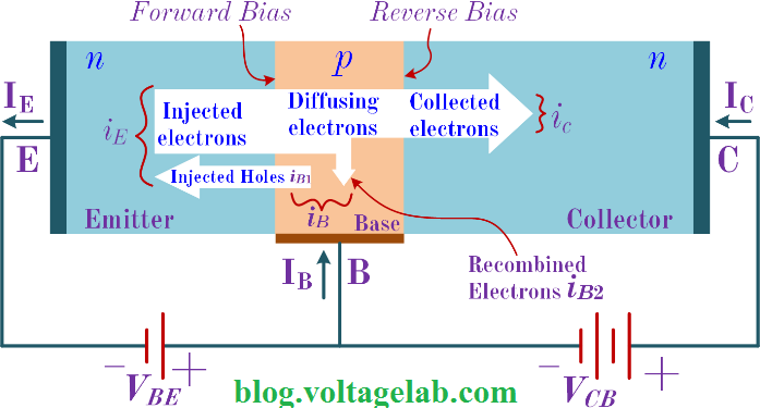
The figure shows two voltage sources (VBE & VCB) which are connected to bias the transistor. VBE is the base-emitter voltage, providing forward bias to the junction, while VCB provides reverse bias to the collector-base junction.
As the base-emitter junction is forward biased, many electrons from the n-type emitter cross the base-emitter junction and diffuse into the p-type base region, resulting in emitter current IE.
Since the base layer is a thinly doped p-type semiconductor, it has a small number of majority carriers, which are holes. A small number of these holes form base current iB1 as they move from the emitter region.
Some of the base holes combine with a very small number of electrons coming from the emitter, causing electron-hole recombination, leading to a small base current iB2. Hence, the base current IB has two components: iB1 and iB2.
The large number of electrons entering the base are considered minority carriers. As we know, current flows through a PN junction for minority carriers in reverse bias.
Since the base-collector junction is reverse biased, many electrons from the p-type base cross the base-collector junction and are collected by the n-type collector region. They are attracted to the positive terminal of the VCB source, creating collector current IC.
This is how current flows through an NPN transistor via electron movement. In the figure, the directions of currents IE, IB, and IC are shown, which are opposite to the direction of electron flow. By applying KCL at the base point of the transistor, we get:
IE = IB + IC. All the current flows out of the transistor through the emitter terminal.
Let’s explain it in simpler terms:
- Current sent through the base exits through the emitter.
- The transistor pulls current from the collector to the emitter, resulting in current flow from collector to emitter.
- The base-emitter current IB controls the collector-emitter current IC.
- The collector-emitter current is much larger than the base-emitter current.
- The base-emitter connection acts like a diode.
- The transistor turns on when the base-emitter voltage reaches 0.7 volts.
- This results in the flow of current through both the base-emitter and collector-emitter paths.
- This voltage is called the threshold voltage or turn-on voltage, where the transistor activates.
The operation of a PNP transistor is the opposite of an NPN transistor. If you understand NPN operation, PNP operation should be easier to grasp.
Where Are Transistors Used?
- As switches: Used in solid-state relays.
- As amplifiers: Used to amplify current or voltage.
- As regulators: Used to regulate current, voltage, and power.
- As buffers: Used for impedance matching.
Overview of Transistor
The base-emitter junction’s resistance is lower than that of the base-collector junction, so a small forward bias is applied at the base-emitter junction, and a high reverse bias is applied at the base-collector junction.
A transistor has a base, emitter, and collector.
The base layer is very thin, the emitter is of medium thickness, and the collector layer is the thickest.
The emitter is highly doped to supply the maximum majority carriers to the base layer.
The base-emitter junction is always forward biased, while the base-collector junction is always reverse biased.
What is a transistor?
A transistor is a semiconductor device with three terminals that can amplify signals or act as a switch. It is a fundamental building block of modern electronic devices.
What are the main types of transistors?
The main types of transistors are Bipolar Junction Transistors (BJTs), which include NPN and PNP transistors, and Field-Effect Transistors (FETs), such as MOSFETs.
What is the primary purpose of a transistor?
The primary purpose of a transistor is to amplify electrical signals or act as a switch in electronic circuits. This allows for the control and modification of signal strength and electrical power in various applications.
How does a transistor operate?
A transistor works by controlling the flow of electrical current between its terminals. In an NPN transistor, a small current at the base terminal allows a larger current to flow between the collector and emitter. In a PNP transistor, the process is reversed, with the direction of current flow being different.
What is an NPN transistor?
An NPN transistor has an N-type semiconductor as the emitter and collector, with a P-type semiconductor as the base. It amplifies current flowing into the base to a larger current flowing from the collector to the emitter.
What is a PNP transistor?
A PNP transistor has a P-type semiconductor as the emitter and collector, with an N-type semiconductor as the base. It amplifies current flowing out of the base to a larger current flowing from the emitter to the collector.
