

The full form of BJT is Bipolar Junction Transistor, where Bipolar refers to both electrons and holes. Junction means connection, and the word Transistor comes from Transfer + Resistor.
The Bipolar Junction Transistor (BJT) is a fundamental semiconductor device that plays a key role in amplifying weak signals and in switching circuits. With its ability to control current flow through two types of charge carriers, electrons and holes, the BJT is widely used in various electronic applications. In this article, we will explore the physical structure, types, and working principles of BJTs, shedding light on how they transfer resistance and amplify current in electronic circuits.
Study smarter with VoltageLab
Built for electricians, apprentices, and electrical engineers who want faster practice and better exam prep.
⭐️ Join thousands of electricians upgrading their skills
What is a BJT (Bipolar Junction Transistor)?
A BJT is a 3-terminal device used to amplify weak signals and is also used in switching circuits.
Physical Structure of Bipolar Junction Transistor (BJT)
There are generally two types of BJTs:
1) n-p-n type BJT
2) p-n-p type BJT
A BJT is composed of three regions. The first region is called the Emitter (E), the second region is called the Base (B), and the third region is called the Collector (C).
There are two junctions in a BJT. One is between the Emitter and the Base, and the other is between the Base and the Collector.
Now let’s take a quick look at how an n-p-n transistor is made: First, a semiconductor is taken. Then, the Emitter region is doped with 10^19 electrons (-ve), the Base region with 10^14 holes (+ve), and the Collector region with 10^20 electrons (-ve). This is why the Collector region is wider.
How does a BJT work? (Working Principle)
To make any electronic device work, it needs to be powered, meaning it needs to be biased. To bias a BJT, the negative terminal of the first battery is connected to the Emitter terminal of the Bipolar Junction Transistor, and the positive terminal is connected to the Base terminal.
The negative terminal of the second battery is connected to the Base terminal, and the positive terminal is connected to the Collector terminal. (A biasing diagram is provided below)
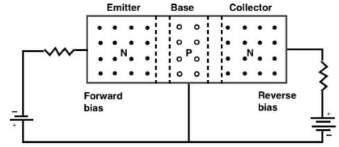
Since the negative terminal of the battery is connected to the Emitter and the positive terminal is connected to the Base, the Emitter and Base are forward biased. Similarly, the Base and Collector are reverse biased. In forward biasing, the depletion region is small, leading to low resistance, while in reverse biasing, the depletion region is large, leading to high resistance.
Notice that the first junction has low resistance, and the second junction has high resistance. This means the Bipolar Junction Transistor transfers resistance. That’s why it is called a Transfer Resistor = Transistor.
Since the negative terminal of the battery is connected to the Emitter, the battery will push the Emitter’s electrons (10^19 electrons) forward, causing them to move ahead and creating Emitter current (IE).
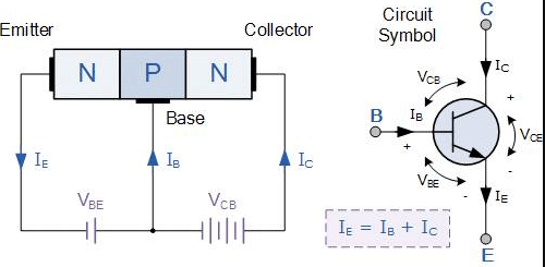
As the electrons move forward, they meet the 10^14 holes in the Base region and neutralize them. The first battery’s positive terminal will then supply more holes to the Base, generating Base current (IB).
After the Emitter electrons neutralize the 10^14 holes, the remaining electrons (10^19 – 10^14 ≈ 10^19 electrons) will pass through the Collector to the positive terminal of the second battery, generating Collector current (IC).
Here, the Emitter and Collector currents are generated by electrons, while the Base current is generated by holes. Since the current flow is caused by both electrons and holes, it is called Bipolar.
Out of 100% of the Emitter’s electrons, less than 1% are responsible for creating the Base current, while over 99% create the Collector current.
Thus, Emitter current (IE) = Collector current (IC) + Base current (IB).
What are the applications of Bipolar Junction Transistor (BJT)?
BJTs are widely used in amplification circuits, switching applications, and signal modulation. They are essential components in consumer electronics, communication devices, and industrial control systems.
What are the areas of application for power Bipolar Junction Transistors?
Power BJTs are used in high-power applications such as motor controllers, power amplifiers, and switching circuits in power supplies due to their ability to handle large currents and voltages.
What are the advantages of Bipolar Junction Transistors (BJTs)?
BJTs offer high current density, good switching performance, and better amplification characteristics compared to other transistors, making them suitable for both small signal amplification and power applications.
Study smarter with VoltageLab
Built for electricians, apprentices, and electrical engineers who want faster practice and better exam prep.
⭐️ Join thousands of electricians upgrading their skills
What are the applications of power Bipolar Junction Transistors?
Power BJTs are commonly applied in power regulation, energy conversion systems, motor drives, and high-power switching circuits.
How is a Bipolar Junction Transistor (BJT) used as a switch?
In switching applications, a BJT operates in saturation mode (ON state) and cut-off mode (OFF state), allowing it to function as an efficient switch in digital circuits.
How does a Bipolar Junction Transistor (BJT) amplify a signal?
BJTs amplify signals by controlling the current flow through the base-emitter junction, where a small input current in the base leads to a larger output current in the collector, thus amplifying the signal.
What is active mode in a Bipolar Junction Transistor (BJT)?
In active mode, the BJT operates with the base-emitter junction forward biased and the base-collector junction reverse biased, allowing the transistor to function as an amplifier.
What is the basic principle of a Bipolar Junction Transistor (BJT)?
The basic principle of a BJT is to control the flow of current between the collector and emitter by varying the small current at the base, allowing it to function as both an amplifier and a switch.
What are the basic types of Bipolar Junction Transistors (BJTs)?
There are two basic types of BJTs: NPN and PNP transistors, differentiated by the arrangement and flow of charge carriers (electrons and holes).
Practice more with electrical quizzes
NEC · BS7671 · AS/NZS · CEC · DIN VDE
